- 您现在的位置:买卖IC网 > Sheet目录3818 > PIC18F4620-I/ML (Microchip Technology)IC MCU FLASH 32KX16 44QFN
2008 Microchip Technology Inc.
DS39626E-page 19
PIC18F2525/2620/4525/4620
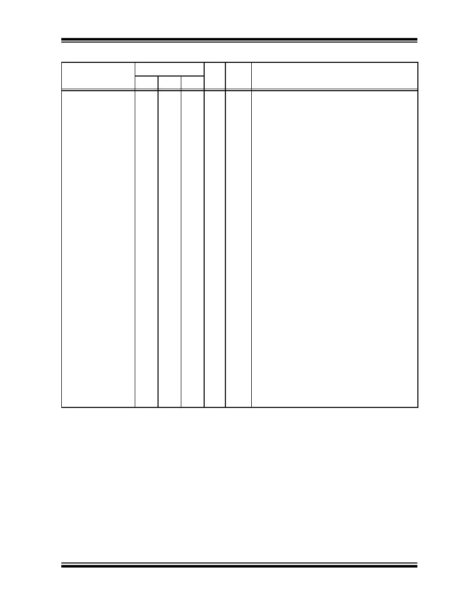
PORTC is a bidirectional I/O port.
RC0/T1OSO/T13CKI
RC0
T1OSO
T13CKI
15
34
32
I/O
O
I
ST
—
ST
Digital I/O.
Timer1 oscillator output.
Timer1/Timer3 external clock input.
RC1/T1OSI/CCP2
RC1
T1OSI
CCP2(2)
16
35
I/O
I
I/O
ST
CMOS
ST
Digital I/O.
Timer1 oscillator input.
Capture 2 input/Compare 2 output/PWM2 output.
RC2/CCP1/P1A
RC2
CCP1
P1A
17
36
I/O
O
ST
—
Digital I/O.
Capture 1 input/Compare 1 output/PWM1 output.
Enhanced CCP1 output.
RC3/SCK/SCL
RC3
SCK
SCL
18
37
I/O
ST
Digital I/O.
Synchronous serial clock input/output for
SPI mode.
Synchronous serial clock input/output for I2C
mode.
RC4/SDI/SDA
RC4
SDI
SDA
23
42
I/O
I
I/O
ST
Digital I/O.
SPI data in.
I2C data I/O.
RC5/SDO
RC5
SDO
24
43
I/O
O
ST
—
Digital I/O.
SPI data out.
RC6/TX/CK
RC6
TX
CK
25
44
I/O
O
I/O
ST
—
ST
Digital I/O.
EUSART asynchronous transmit.
EUSART synchronous clock (see related RX/DT).
RC7/RX/DT
RC7
RX
DT
26
1
I/O
I
I/O
ST
Digital I/O.
EUSART asynchronous receive.
EUSART synchronous data (see related TX/CK).
TABLE 1-3:
PIC18F4525/4620 PINOUT I/O DESCRIPTIONS (CONTINUED)
Pin Name
Pin Number
Pin
Type
Buffer
Type
Description
PDIP
QFN
TQFP
Legend: TTL = TTL compatible input
CMOS = CMOS compatible input or output
ST = Schmitt Trigger input with CMOS levels
I
= Input
O
= Output
P
= Power
Note 1:
Default assignment for CCP2 when the CCP2MX Configuration bit is set.
2:
Alternate assignment for CCP2 when the CCP2MX Configuration bit is cleared.
3:
For the QFN package, it is recommended that the bottom pad be connected to VSS.
发布紧急采购,3分钟左右您将得到回复。
相关PDF资料
PIC24HJ256GP210-I/PT
IC PIC MCU FLASH 128KX16 100TQFP
PIC24HJ128GP310A-I/PF
IC PIC MCU FLASH 128KB 100-TQFP
DSPIC33FJ128GP310-I/PF
IC DSPIC MCU/DSP 128K 100TQFP
PIC16C66-20I/SO
IC MCU OTP 8KX14 PWM 28SOIC
DSPIC33FJ128MC510-I/PT
IC DSPIC MCU/DSP 128K 100TQFP
PIC16C66-20I/SP
IC MCU OTP 8KX14 PWM 28DIP
PIC18LF2620-I/SP
IC MCU FLASH 32KX16 28SDIP
PIC16F877-04I/P
IC MCU FLASH 8KX14 EE 40DIP
相关代理商/技术参数
PIC18F4620-I/P
功能描述:8位微控制器 -MCU 64KB 3968 RAM 36 I/O RoHS:否 制造商:Silicon Labs 核心:8051 处理器系列:C8051F39x 数据总线宽度:8 bit 最大时钟频率:50 MHz 程序存储器大小:16 KB 数据 RAM 大小:1 KB 片上 ADC:Yes 工作电源电压:1.8 V to 3.6 V 工作温度范围:- 40 C to + 105 C 封装 / 箱体:QFN-20 安装风格:SMD/SMT
PIC18F4620-I/P
制造商:Microchip Technology Inc 功能描述:IC 8BIT FLASH MCU 18F4620 DIP40
PIC18F4620-I/PT
功能描述:8位微控制器 -MCU 64KB 3968 RAM 36 I/O RoHS:否 制造商:Silicon Labs 核心:8051 处理器系列:C8051F39x 数据总线宽度:8 bit 最大时钟频率:50 MHz 程序存储器大小:16 KB 数据 RAM 大小:1 KB 片上 ADC:Yes 工作电源电压:1.8 V to 3.6 V 工作温度范围:- 40 C to + 105 C 封装 / 箱体:QFN-20 安装风格:SMD/SMT
PIC18F4620-I/PT
制造商:Microchip Technology Inc 功能描述:IC 8BIT FLASH MCU 18F4620 TQFP44
PIC18F4620T-I/ML
功能描述:8位微控制器 -MCU 64KB 3968 RAM 36 I/O RoHS:否 制造商:Silicon Labs 核心:8051 处理器系列:C8051F39x 数据总线宽度:8 bit 最大时钟频率:50 MHz 程序存储器大小:16 KB 数据 RAM 大小:1 KB 片上 ADC:Yes 工作电源电压:1.8 V to 3.6 V 工作温度范围:- 40 C to + 105 C 封装 / 箱体:QFN-20 安装风格:SMD/SMT
PIC18F4620T-I/PT
功能描述:8位微控制器 -MCU 64KB 3968 RAM 36 I/O RoHS:否 制造商:Silicon Labs 核心:8051 处理器系列:C8051F39x 数据总线宽度:8 bit 最大时钟频率:50 MHz 程序存储器大小:16 KB 数据 RAM 大小:1 KB 片上 ADC:Yes 工作电源电压:1.8 V to 3.6 V 工作温度范围:- 40 C to + 105 C 封装 / 箱体:QFN-20 安装风格:SMD/SMT
PIC18F4680-E/ML
功能描述:8位微控制器 -MCU 64KB 3328 RAM w/ECAN RoHS:否 制造商:Silicon Labs 核心:8051 处理器系列:C8051F39x 数据总线宽度:8 bit 最大时钟频率:50 MHz 程序存储器大小:16 KB 数据 RAM 大小:1 KB 片上 ADC:Yes 工作电源电压:1.8 V to 3.6 V 工作温度范围:- 40 C to + 105 C 封装 / 箱体:QFN-20 安装风格:SMD/SMT
PIC18F4680-E/P
功能描述:8位微控制器 -MCU 64KB 3328 RAM w/ECAN RoHS:否 制造商:Silicon Labs 核心:8051 处理器系列:C8051F39x 数据总线宽度:8 bit 最大时钟频率:50 MHz 程序存储器大小:16 KB 数据 RAM 大小:1 KB 片上 ADC:Yes 工作电源电压:1.8 V to 3.6 V 工作温度范围:- 40 C to + 105 C 封装 / 箱体:QFN-20 安装风格:SMD/SMT